How to Build a $20B Semiconductor Fab
For the last several decades, one avenue of technological progress has towered over nearly everything else: semiconductors. Semiconductors are materials that can have their conductivity varied by many orders of magnitude, which makes it possible to selectively block and allow the flow of electrons. This property makes it possible to manufacture all sorts of electronic devices, not least of which is the digital computer.
As semiconductor technology has advanced over the past several decades, the cost and size of electronic computation has steadily fallen, making the PC, the internet, and mobile phones all possible. Today, semiconductors in the form of powerful GPUs that can perform enormous numbers of matrix multiplications are the keystone for advancing AI technology. Increasingly available computation to do enormous amounts of search and learning drives progress in things like game-playing AI, computer vision, and large language models (LLMs).
As Moore’s Law has marched forward, transistors (an electronic switch which is the fundamental building block of integrated circuits) have gotten smaller and cheaper. In 1954, the first transistor radio, the TR-1 had 4 transistors which cost $2.50 apiece ($29.03 in 2024 dollars). Today, an AMD Ryzen processor with 9.9 billion transistors is on sale for $650, or about $0.000000066 per transistor; in other words, since the 1950s the cost of a transistor has fallen by about a factor of 300 million.
The same shrinking and cheapening has happened for every semiconductor component. But at the same time, the facilities to manufacture them have become increasingly expensive. In the late 60s and early 70s, a semiconductor fabrication facility (or ‘fab’) cost on the order of $4 million (~$31 million in 2024 dollars). Today, a modern fab can cost $10-$20 billion or more. Intel is building a pair of fabs in Arizona which are projected to cost $15 billion apiece, and Samsung’s fab in Taylor, Texas is projected to cost $25 billion.

These enormous costs are ultimately due to the same factor that has steadily driven down the cost of semiconductors: Moore’s Law, the observation that the number of components on an integrated circuit tends to double every two years. (There is a Moore’s Second Law, also known as Rock’s Law, which posits that the cost of a semiconductor fab doubles every four years.) The smaller semiconductor components get, the more difficult it is to create the conditions to manufacture them.
A modern microchip has features on the order of 50 nanometers in width, or around 1/2000th the width of a human hair.1 Materials are placed in layers a few atoms thin. Creating objects this small requires ultra-precise manufacturing equipment, and a production environment that can screen out as many sources of interference as possible; every rogue speck of dust or tiny fluctuation in electrical voltage. And these conditions must be maintained not in the rarefied conditions of an experimental lab, but in a mass production facility that is producing hundreds of millions of microchips every year. The combination of ultra-precision and high-volume production results in some of the most complex, expensive factories in the world.
To understand why a modern fab is so expensive, we first need to understand the process for manufacturing semiconductors.
If we sliced a computer chip down the middle, and looked very, very closely, we would see that it is composed of a series of layers. Here is a cross section of a chip made with Intel’s current manufacturing process:
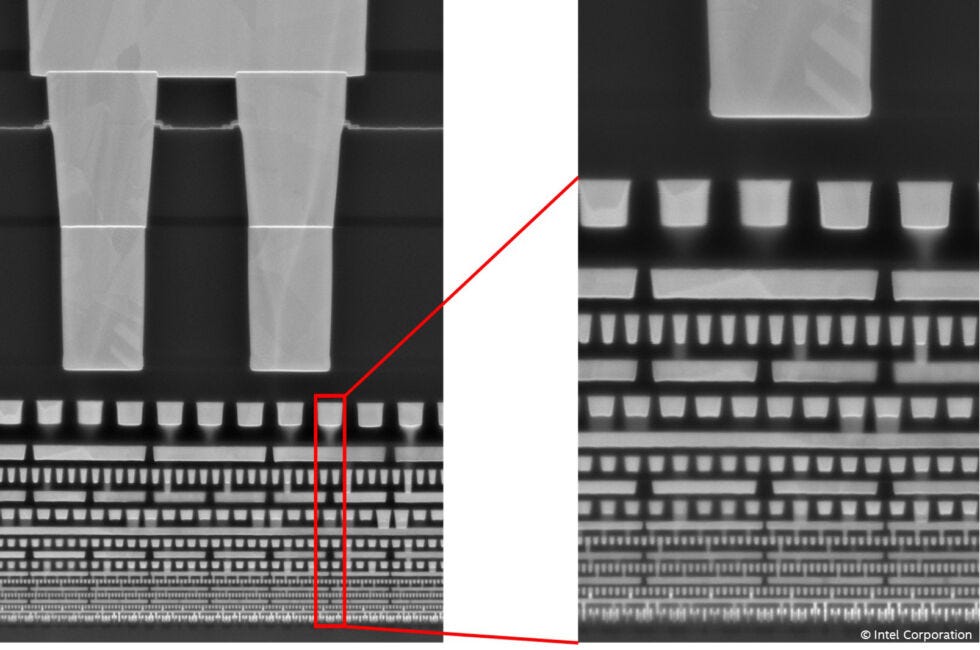
And here’s an illustrated cross section of a generic integrated circuit, showing the different layers:

At the bottom of the chip, the area marked FEOL (front end of line) on the graphic above are the semiconductor components themselves: transistors, capacitors, resistors, diodes, and all the other parts created out of silicon to make a microchip.2 These individual components will be connected together using microscopic metal wires, the layers in the area marked BEOL (back end of line). Because of the enormous number of components in a modern electronic chip, this wiring must be routed on separate layers, which are separated by electrical insulators known as dielectrics. Intel’s current process, for instance, consists of 15 layers of metal wiring. This wiring gets connected together and to the semiconductor components through holes in the layers known as ‘vias.’
Chips are made by building up this complex structure one layer at a time. Starting with a wafer of extremely pure silicon, layers of material are added, portions of the layer are removed, more material is added (or existing material is modified), and so on, until the entire structure is complete. This fabrication method is known as the planar process, and it was invented at Fairchild Semiconductor in 1959 by Jean Hoerni. It’s what makes integrated circuits, and modern computer technology, possible.
The process for building up the structure of a microchip can be broken down into four basic operations, repeatedly applied: layering, patterning, doping, and heat-treating.
Layering
Layering is used to add an extremely thin layer of material — as little as a nanometer or less, 1/100,000th the thickness of a human hair — to the surface of the wafer. These layers might be insulators (such as layers of silicon dioxide used to separate components), conductors (such as layers of copper wiring used to connect components) or semiconductors (such as epitaxial thin films of silicon which form part of the semiconductor components). Depending on the step in the process and the material being used, different layering techniques might be applied.
Deposition methods have also evolved over time as features have shrunk. Current common layering methods include thermal oxidation (exposing wafers to oxygen in a furnace, which creates a thin layer of silicon dioxide on the wafer surface), chemical vapor deposition (CVD) (where gaseous chemicals are brought together, depositing their reactants on the surface of the wafer) and sputtering (where a solid material is bombarded with plasma ions, causing atoms to break free and be deposited on the wafer’s surface). The small size of modern semiconductor components demands that these layering methods are capable of extreme precision; modern atomic layer deposition methods, for instance, are capable of creating a single layer of atoms at a time.
Patterning
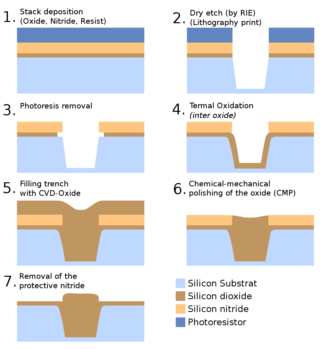
Patterning is the process of inscribing specific patterns on the wafer, selectively removing material as needed to create electronic components. On modern semiconductors this is done using photolithography. A wafer is first coated with a thin layer of light-sensitive material called photoresist. Bright light of a specific wavelength is shone through a glass or quartz plate called a mask that has the pattern to be created on the wafer inscribed on it. A mask contains the patterns necessary for a single chip, but a wafer will contain hundreds of individual chips. To expose each one, the mask is moved back and forth over the surface of the wafer using a stepper or scanner. The light that isn’t blocked by the mask passes through and induces a chemical reaction in the photoresist; with positive photoresist, the area exposed to light weakens and becomes soluble; with negative photoresist, the exposed area hardens while the rest of the photoresist remains soluble. In either case, the wafer will be washed after it’s exposed to light, leaving behind a hardened layer of photoresist in the pattern that needs to be applied.
From here, the wafer will be etched: a corrosive chemical will be applied to the wafer, eating away the material exposed by the removed photoresist and inscribing the pattern onto the wafer itself. Etching can be “wet” (by exposing the wafer to liquid chemicals such as hydrofluoric acid) or “dry” (by exposing the wafer to gasses like fluorine which have been energized into a plasma). After etching, the remaining photoresist is removed.
Doping
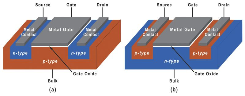
Doping is the process of introducing very small amounts of impurities into a semiconductor material to change its electrical conductivity. By doping silicon with a small amount of a group V element, such as phosphorus or arsenic, an n-type semiconductor with an excess of free electrons is created. By doping it with a small amount of a group III element, such as boron, a p-type semiconductor with an excess of electron holes is created. With the proper arrangement of p-type and n-type silicon, components such as transistors can be created.
Early on, the primary method of introducing impurities in semiconductor manufacturing was diffusion: by heating the wafer up in the presence of a gas, atoms of the gas would diffuse into the wafer surface. But today doping is primarily done via ion implantation: a beam of ions (atoms with an excess or deficit of electrons, giving them an electrical charge) is fired at the wafer, depositing the atoms below the surface.

Heating
The last primary operation in semiconductor manufacturing is heating. There are many steps in the process where the wafer is heated or cooled to obtain a specific result. Ion implantation, for instance, results in a damaged silicon crystal structure. This damage is repaired with rapid thermal annealing; thermal lamps heat the wafer to over 1,000 degrees in a matter of seconds, and then the wafer is slowly cooled, repairing the crystal structure. Heating is also used during the lithography process to “bake” and harden the liquid photoresist.

In addition to these four basic processes, semiconductor manufacturing involves many other supporting processes. One key supporting process is polishing: because a microchip is built up from dozens of individual layers, variations in layer thickness will propagate over time as more layers are added, causing problems if left unaddressed. To combat this, wafers are frequently polished during the fabrication process using chemical mechanical polishing (CMP) to smooth out the wafer surface. CMP is also used to fill holes created by etching, by applying a layer of material to the entire wafer and then polishing away the material above the hole.

Another key supporting process is cleaning. Because the tiniest stray particle can cause a microchip to malfunction, wafers must be constantly cleaned with solvents and extremely pure water. In a modern fab, a wafer might get cleaned 200 times or more during the production process. And to ensure that processes are working correctly, fabs make extensive use of metrology — measuring the wafer at various points in the process to determine if there have been any manufacturing mistakes or defects.

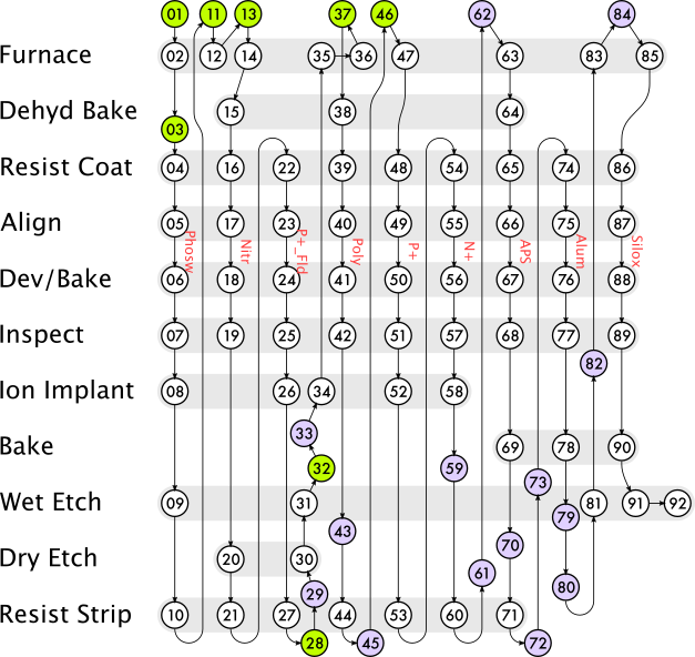
By applying these four basic processes over and over again, along with the various support processes, the structure of a microchip is slowly built up. And as more transistors have been crammed onto an integrated circuit, this structure (and the process for creating it) has become increasingly complex. Early integrated circuits could be made with just five to ten different masks and dozens of process steps, but a modern leading-edge microchip might require 80 or more masks and thousands of separate process steps.
Once the wafer has gone through all these steps and the structure of the circuit is complete, it proceeds to assembly and packaging. This is where the wafers are cut apart into individual chips, each chip is connected to wires (and to any other chips, as with advanced packaging) and is encased in a protective coating. Packaging might be done at the semiconductor fab, or at another facility entirely.
On its own, a large number of process steps wouldn’t require $20 billion manufacturing facilities. After all, many complex manufactured goods require as many or more steps to produce. An early 20th century watch, for instance, consisted of 150 parts that required over 3700 operations to produce.
But when these process steps are being used to make components whose size is measured in the billionths of a meter, manufacturing complexity is enormously magnified. With most manufacturing processes, even those using precision methods to produce interchangeable parts, there is a fair degree of tolerance in the process. If a part is a fraction of a millimeter too long or too short, it will still fit. If the impurity content of a metal is a tiny bit too high, the metal can still be used. If a process runs slightly too fast or too slow, the output is still usable.
In semiconductor manufacturing, allowable tolerances are whittled away to almost nothing. Making transistors a few nanometers across requires processes that are hundreds of thousands of times more accurate than conventional manufacturing. The tiniest rogue particle can short out a connection and destroy an entire chip. A few atoms in the wrong place can cause a process step to fail. Imperceptibly small amounts of impurities can irreparably damage materials.

The history of semiconductor manufacturing is a chronicle of an endless war against these minute effects and their catastrophic impacts. Even getting semiconductor devices to work at all required paying extremely close attention to chemical concentrations and rogue impurities. When semiconductors were being researched at Bell Labs in the 1940s, mysterious component failures were eventually traced to researchers who had touched copper door knobs; the tiny number of copper atoms that migrated from the door to the workers hands was enough to ruin their work material. Early semiconductor manufacturers found that their processes were influenced by, among other things, the phase of the moon, whether workers had recently visited the bathroom, and female workers’ menstrual cycles.
And as semiconductor features have gotten smaller, the problem has only gotten more difficult. As transistors shrank, Intel found that even the most innocuous equipment change — using a slightly longer pipe or cable, for instance — could cause process disruptions to new fabs and cause months or years of lower yields. To combat this, Intel instituted a process known as Copy EXACTLY! New fabs would be identical to existing fabs to the extent possible, right down to the color and brand of the paint on the walls.
A modern semiconductor fab must thus create a world of incredible precision and predictability. Every possible effect that might disrupt the manufacturing process, no matter how small, must be screened off, any subtle deviation hunted down and eliminated. And this control must be maintained in a mass production environment, where hundreds of thousands of wafers and millions of individual chips (each one with billions of transistors) are produced each year.
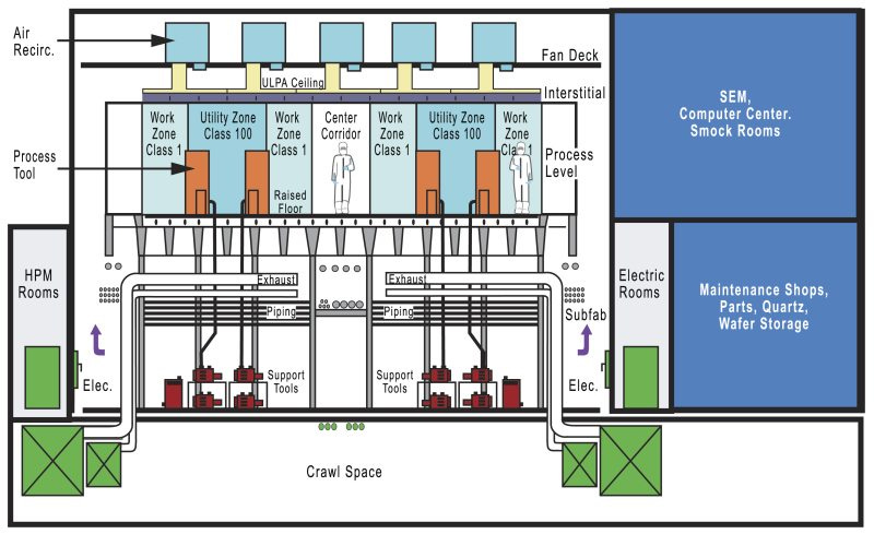
To create this environment, a modern semiconductor fab typically consists of four levels. The heart of the fab is the cleanroom level; the factory floor where the fabrication process actually takes place. Below the cleanroom is the sub-fab, one or more levels (typically two) that contain the ducts, piping, wiring, and equipment needed to support the cleanroom operations. And above the cleanroom level is an interstitial space with fans and filters used for recirculating air into the cleanroom below.
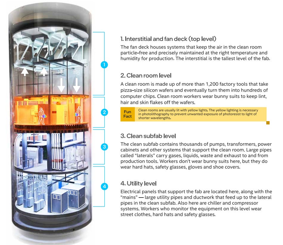
The cleanroom level contains the process tools: the individual pieces of equipment that perform the various operations discussed above. Tools range from lithography machines (such as ASML’s EUV machines), to chemical vapor deposition machines, to ion implanters, to “wet benches” for cleaning and etching, and so on. These machines are made by a small handful of specialty manufacturers such as ASML, Lam Research, Applied Materials, and Tokyo Electron, and are incredibly expensive. Major process machines can cost $5-$10 million, and some can cost upwards of $100 million. ASML’s cutting edge photolithography machines cost nearly $400 million.
These tools might perform one specific process step (such as furnaces for wafer heating) or integrate several individual process steps. Applied Materials, for instance, makes machines which incorporate multiple layering and surface preparation steps. To produce a large number of wafers (a modern microprocessor or “logic” fab might produce 40 to 50,000 wafers a month; a fab producing memory might produce 120,000), a large number of tools are required, 1,000 or more.
Process tools will be clustered together by type; this allows the tools to share requirements for things like chemical and gas lines (it’s easier to run piping if all the demand for a certain chemical is in one place), and it makes it possible to isolate certain contaminants. Since copper impurities can have catastrophic effects on semiconductor behavior, parts of the process that use copper (such as the tools depositing microscopic copper wiring) might be isolated from other parts of the fab. HVAC systems will similarly be isolated between different process zones. To minimize interference from things like columns or load-bearing walls, the roof of the fab is typically supported by large, long-spanning trusses which allow the cleanroom space to be as open as possible.

The cleanroom is designed to minimize contamination. Semiconductor fabs are typically built with Class 10 or Class 100 cleanrooms, meaning there can be a maximum of 10 or 100 particles 0.5 microns or larger in each cubic foot of air. By comparison, an ordinary house has on the order of 500,000 particles per cubic foot of air, and a surgical operating room will have about 100,000.) To achieve this, large air handling units force air down through HEPA or ULPA filters in the cleanroom ceiling. The air is pulled down through the floor into the sub-fab, then recirculated up through the ceiling over and over again.
To prevent particles outside the cleanroom from entering, the cleanroom is kept at positive pressure relative to the outside. Keeping the air at the level of cleanliness required means the air is being changed hundreds of times per hour, compared to the 5-10 times per hour in a typical office building. This volume of air flow, combined with the size of semiconductor cleanrooms (which might be 500,000-1M square feet or more on large fabs), means that fab HVAC systems are enormous.
In addition to these large HVAC systems, the materials and process tools used in the cleanroom need to be specially designed not to emit particles. To minimize contamination from people inside the cleanroom, workers don bunny suits in a special gowning area before entering, and go through a special cleaning procedure.
As semiconductor features shrank, cleanroom requirements became more stringent. In the 1980s fab cleanrooms were being built to Class 1000 standards, but by the 1990s, some manufacturers were building incredibly clean Class 1 cleanrooms (just one 0.5 micron particle per cubic foot of air). Because achieving this level of cleanliness is costly, manufacturers have adopted a strategy of isolating the wafers from the rest of the cleanroom. Wafers are transported between process tools in sealed pods called FOUPs (front opening unified pods), and the process tool itself is enclosed and sealed off. This TSMC fab, for instance, was built with a Class 100 cleanroom, but the wafers themselves are handled inside Class 0.1 “mini-environments.” By adopting the mini-environment strategy, fabs have been able remove even more impurities from the air without having to purify the millions of cubic feet of air in the cleanroom.

FOUPs are moved between process tools using an automated material handling system. In most modern fabs, this consists of a ceiling-mounted rail system (though some fabs, particularly older ones, may use floor-based automated guided vehicles instead). Specially designed vehicles pick up FOUPs at one process tool, and drop them off at the next one. The large number of manufacturing steps means that it can take months for a wafer to go through the entire process. This, combined with the large number of wafers a fab produces a month, means that at any given time there are tens of thousands of wafers at various points in the production process, traveling back and forth between tools or being stored waiting for their turn. Over the course of the production process a wafer will travel many miles back and forth between different production tools. Because of this, the rail transport systems must be extensive, with miles of track and hundreds or thousands of transport vehicles. And they must be carefully designed to avoid bottlenecks and allow the “traffic” to flow smoothly.

When it arrives at the process tool, the FOUP can be connected to a special loading point, and wafers can be handled automatically within the controlled environment of the machine. After processing, the wafer can be loaded into another FOUP and moved on to the next tool. Since a process tool may not be available immediately, FOUPs are kept in storage until a spot opens up and they can be moved. FOUPs in storage will be occasionally flushed with nitrogen to ensure no contaminants reach the wafers inside.3
But rogue particles aren’t the only thing that can disrupt the manufacturing process, and every part of the fab, from the cleanroom down to the foundation, must be designed to minimize outside interference. The extreme precision required means process tools are extremely sensitive to vibration (even loud noises can negatively affect the manufacturing process), and fabs are designed to minimize it. Fabs are typically built away from airports, rail lines, busy highways, and any other significant outside source of vibrations, and the fab supporting facilities themselves must also be designed to eliminate vibrations. (In one case, unacceptable cleanroom floor vibrations were being caused by an exhaust vent 400 feet away from the fab building.) This extreme vibration sensitivity is exacerbated by the enormous amount of potentially vibration-generating machinery and equipment in a fab such as motors, pumps, HVAC systems, and even fluid flow in pipes. Fabs must limit vibrations to several orders of magnitude below the threshold of perception, while simultaneously absorbing 100 times the mechanical energy and 50 times the air flow as a conventional building.

To minimize vibrations, the floor of the cleanroom is typically built as a deep concrete waffle slab two to four feet thick, supported by closely spaced columns to make it as stiff as possible. Above the slab is a raised metal flooring which allows pipes and cables to be routed below it, and allows process tools to be placed on separate supporting pedestals to prevent worker footsteps from causing vibrations. Some extremely sensitive equipment, such as lithography tools, might require even more stringent measures like active vibration dampers that can sense and cancel out any rogue vibrations. In some cases a fab might be built with a structural isolation break to keep the cleanroom floor physically separated from the rest of the building and any vibrations it might induce.


Preventing vibration also means, ideally, placing your fab in a seismically inactive area. When this isn’t possible (such as in Taiwan or Japan), other measures might be taken, such as adding earthquake dampers or using special foundations that isolate the building from the surrounding soil.
In addition to particles and vibrations, there are numerous other sources of interference a fab is designed to eliminate. To prevent light from accidently exposing photoresist, lithography areas often use special yellow lights that won’t expose the chemicals. Anti-static materials must be used for things like flooring to prevent the buildup of static electricity. Tools are sensitive to electromagnetic interference (even the fields from nearby power lines might cause equipment disruption), and tools must be shielded and EMF sources minimized. Fabs have backup generators and uninterruptible power supplies in case of power outages, and equipment must be designed to handle the voltage variations in utility electricity supply. (Prior to design standards that required this, it was apparently common for utility voltage variations to cause semiconductor manufacturing issues.) Temperature and humidity in the cleanroom must be maintained in a narrow range, which places further burden on the HVAC system. A fab also may be designed to be radiofrequency (RF) shielded for security purposes.
Beneath the carefully controlled conditions of the cleanroom lies the sub-fab: one or more levels of equipment needed to support the operations of the cleanroom. An EUV lithography machine, for instance, is a complex piece of equipment the size of a truck, but the cleanroom tool is only a portion of the total equipment required. Beneath the cleanroom lies the enormous CO2 laser that drives the EUV system, and the pumps required to create the vacuum within the process chamber. Many other process tools, such as ion implanters and sputtering machines, also require a vacuum, and a large fab may have thousands of vacuum pumps in the sub-fab.
The sub-fab is also where many of the chemicals required for process tools are stored and routed (although some chemicals, particularly highly toxic ones, will be stored within the process tools to minimize the risk of leaks, while others will be stored outside the fab building). A semiconductor fab uses a wide variety of chemicals, ranging from nitrogen (used for purging and cleaning FOUPS and process tools), oxygen (used in oxidation furnaces and abatement equipment), argon (used in plasma reactions), hydrogen (used in EUV machine cleaning) and others. The volume of chemicals and gasses used, and the amount of exhaust generated, requires an enormous amount of piping, with some pipes reaching up to ten feet in diameter. And these chemicals must be extremely pure, in some cases 99.9999999% pure.


Many of the chemicals used in the fab, such as phosphine and arsine for doping, are highly toxic. Others, such as the silane used in some CVD processes, are pyrophoric (meaning they ignite spontaneously with air.) One chemical, the chlorine trifluoride used for cleaning CVD chambers, is so toxic and so prone to spontaneous ignition (it's capable of setting wet sand on fire) that some chemists refuse to work with it. These chemicals require special handling and leak detection systems, backup power systems, and specially designed fire protection systems due to the hazard they represent.
The sub-fab also contains the exhaust systems for handling the various byproducts generated by the process tools. To prevent byproducts (particularly ammonia) from reacting with each other, several separate exhaust systems must be used. Many of the processes require abatement equipment (which will burn off any harmful byproducts) or scrubbers to remove hazardous material. This equipment might be mounted to the process tool itself, or be part of a centralized exhaust system.
In addition to chemical handling and exhaust equipment, the sub-fab contains electrical boxes, transformers, fans, air handlers, chillers, RF generators, heat exchangers, and all the other equipment needed to keep the fab tools operating. Sub-fabs are often divided into a “clean” sub-fab (where the air from the cleanroom recirculates), and a separate “dirty” or utility sub-fab below that. And while the level of control can be relaxed somewhat in the sub-fab (workers don’t need to wear bunny suits in it), variations and potential disruptions must still be minimized. Even slight changes in voltage, pressure, or vibration, or the smallest particle emitted by the piping, can negatively affect the manufacturing process.
Achieving this means that sub-fab equipment must be manufactured with much more stringent requirements and much tighter tolerances than in conventional manufacturing. Things like pipes, ducts, pumps, and other material handling equipment are stainless steel and teflon-coated. The interior of pipes must be electropolished to prevent particles from being emitted or providing places for contaminants to accumulate, and pipes must be joined using special orbital welding methods to prevent leaks or contamination. Often sub-fab equipment and material must itself be manufactured in a cleanroom using specialized manufacturing procedures, and transported to the jobsite double-wrapped in plastic bags to prevent contamination during transport. All chemical and gas piping and handling systems must be designed to deliver a smooth, uninterrupted flow of material; even slight variations in pressure can have “disastrous” effects on the production process.
Outside of the sub-fab, many other facilities are required to support cleanroom operations. Moving heavy process tools into the cleanroom requires industrial elevators that can lift tens of thousands of pounds. A fab uses nitrogen and oxygen in such large amounts (a large logic fab might use 50,000 cubic meters of nitrogen every hour) that fabs will often have air separation plants on-site that produce gasses like nitrogen, oxygen and argon. Similarly, a fab will use very large amounts of ultrapure water for wafer cleaning and CMP, along with the regular water for things like chillers for process cooling. A large fab can use millions of gallons of ultrapure water a day, as much as a town of 50,000 people, and producing it requires its own specialized plant. As with other aspects of the fab, the requirements for ultrapure water have gotten more stringent as features have shrunk. Other fab support equipment includes boilers, chillers, emergency generators, and wastewater treatment.

All this equipment and processes consume large amounts of energy. A large fab might demand 100 megawatts of energy, or 10% of the capacity of a large nuclear reactor. Most of this energy is used by the process tools, the HVAC system and other heating/cooling systems. The demands for power and water are severe enough that some fabs have been canceled or relocated when local utilities can’t guarantee supply. And to ensure the proper conditions are maintained in the fab, tens of thousands of sensors are used for monitoring things like particle levels, pressures, and impurity levels.
A large fab will have hundreds of thousands of square feet of cleanroom, and the facility might be spread over hundreds of acres. Building it requires tens of thousands of tons of structural steel, and hundreds of thousands of yards of concrete. Intel boasts that its fabs use twice the concrete as the Burj Khalifa, and five times the metal used in the Eiffel Tower.
Putting this material in place at the necessary level of precision requires thousands of specially trained construction workers. Intel’s new fab in Magdeburg is expected to require over 9,300 workers at its peak, and TSMC’s new fab being built in Arizona is using 12,000. Workers must follow specially-designed “clean construction” protocols to keep materials clean, minimize particle intrusion and to ensure the cleanroom can operate successfully when it's completed. In some cases this has meant things like using equipment to “eat” welding smoke, and painting the edges of anything cut on-site with epoxy paint to prevent particle emissions. To meet the level of cleanliness and precision required, piping and mechanical equipment might be prefabricated off-site and then delivered and installed. To help clarify requirements, SEMI, a semiconductor industry association, publishes numerous standards and design guides on various aspects of facility design and equipment production.
Once the fab is complete to the point where positive pressure can be maintained in the cleanroom (known as “blow down”), the process tooling can be installed. Equipment might arrive in many separate pieces and need a long and careful assembly process — one of ASML’s advanced EUV machines “ships in 40 freight containers, spread over 20 trucks and three cargo planes.” Tools must be handled carefully: the sensitivity of production tools means that a dropped or bumped piece of equipment can result in delays and millions of dollars of repair. And once tooling is installed, it might take six months to a year of ramp up before the fab is hitting acceptable process yields.
Despite their size and complexity, fabs are built surprisingly quickly, around two to four years on average. This is not all that different from other large commercial building projects, and far faster than some other tightly controlled process facilities, like nuclear power plants.
In the US, however, fabs are built slower than elsewhere in the world. Fab construction time in the US has increased from just over 650 days on average in the 1990s to over 900 days on average in the 2010s, compared to around 600-700 days in Asian countries, in part because of increasingly stringent environmental review processes. US fabs are also more expensive to build than in other parts of the world, with estimates ranging from 30% more expensive (per Intel) to up to four times as expensive (per TSMC).4
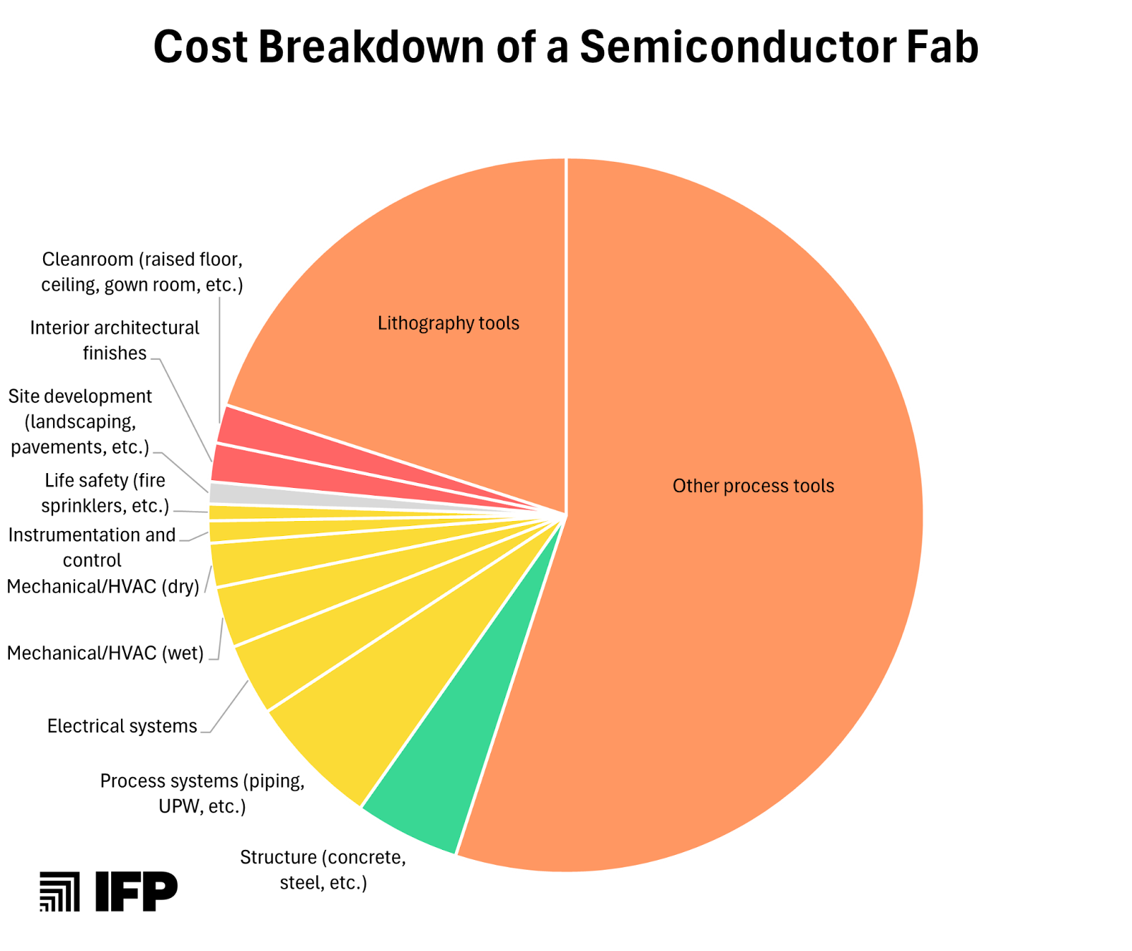
It's not surprising that building fabs is so expensive: they’re large, complicated, and have extremely stringent performance requirements. But the fab exists to provide the necessary environment for the thousands of process tools to function, and it's these tools that are by far the most expensive part of building a new fab. Roughly 70-80% of the cost of a new fab will be the process tools that go in it. (One side effect of this is that upgrading an existing fab to use a more advanced process node can cost an appreciable fraction of the cost of a totally new fab.)
The equipment proportion of fab cost has risen over time. DRAM fabs in the mid-1980s, for instance, were roughly equally split between facilities and equipment cost, but by the late 1990s equipment made up the vast majority of the cost.

For the cost of construction, we see a somewhat similar breakdown as the cost of single family homes, with line items for the structure, architectural finishes, sitework and landscaping, and services and mechanical systems. The main difference is that a fab has a much higher fraction of mechanical, electrical and other services. Things like ultrapure water facilities, multiple exhaust systems, and enormous HVAC needs mean that services make up close to 2/3rds of the cost of a new fab, compared to less than 20% of the cost in a single family home.
For the cost of equipment, the largest expense will typically be the lithography machines followed by equipment for deposition and cleaning and etching. The cost of lithography machines is often estimated as 20% of the cost of a new fab, which means that lithography tools can cost as much as the entire fab facility itself.
As time has gone on and transistors have shrunk, the cost to build a fab has risen. For modern semiconductor fabs, each new process node increases fab cost by about 30%. There are two main drivers of this increase. One is that more advanced process nodes require more expensive equipment. ASML’s EUV lithography machines, for instance, are far more expensive than the deep ultraviolet machines that they replaced. The second main cost driver is that as transistors continue to shrink, more masks and process steps are required to manufacture them. Connecting transistors together requires more layers of metal wires, and FinFETS (transistors made from “fins” that project up from the wafer’s surface) require more layering steps than the simpler transistors they replaced. (EUV, however, temporarily reversed this trend, as it made it possible to do in one mask what previously took two or more, and thus reduced the number of process steps.) More layers and more process steps means more equipment: if product A has twice the manufacturing steps as product B, it will require twice as much equipment to produce if the output level is to remain constant.
But there are also other cost drivers beyond these two factors. As semiconductor features have gotten smaller, the silicon wafers used to produce them have gotten larger. Chips were produced on 50 mm wafers in the 1970s, but today’s leading-edge fabs use much larger 300 mm wafers (a transition to 450mm wafers was planned but never executed), and larger wafers tend to require more expensive equipment. The switch to 300 mm wafers, for instance, necessitated much greater use of automated material handling equipment, as the wafers were too heavy to carry around in FOUPs by hand. These handling systems, in turn, required larger structures with taller cleanroom ceilings.
The ever-increasing cost of fabs has created a shift in the structure of the semiconductor industry. When fabs were cheaper to build, any chip producer could afford to have their own fabs. But as fab costs increased, it became more and more burdensome for manufacturers to operate cutting edge manufacturing facilities due to the high costs, and fewer manufacturers had the production volume to spread those costs over. The “efficient scale” of a 150 mm wafer fab is around 10,000 wafers a month, but for a 300 mm logic wafer fab, that jumps to 40,000 wafers. (And memory wafer fabs will be even larger, at 120,000 wafers per month. Thus only a very small number of companies (currently TSMC, Samsung, and Intel) attempt to operate leading-edge nodes, and the industry has shifted to a “fabless” model where companies like Apple and Nvidia design their chips but have them manufactured by “foundries” like TSMC. By pooling the orders of many different chip companies, the foundries can achieve the scale necessary to afford cutting edge fabs.
The enormous expense of a modern semiconductor fab boils down to the intersection of two things. One is that semiconductor fabs are mass production factories, with modern “gigafabs” producing hundreds of millions of chips per year, each chip containing billions of transistors.5 The second is that producing semiconductors requires almost unfathomable levels of precision. Manipulating huge volumes of matter on the atomic level, repeatedly and reliably, 24 hours a day 365 days a year, is an enormously expensive undertaking.
For those interested in reading more about semiconductor manufacturing, a reading list of the best books and other sources I found on the topic is available here for paid subscribers.